Keynotes

José Lipovetzky
IB, CNEA, CONICET
Monday March 10, 12:00 to 13:00
"Silicon pixelated detectors for gamma and x-rays applications"
In this talk we will explain the basics of ionizing radiation detectors based on silicon pixelated commercial detectors and their application in high resolution x-ray computer tomography among others.
Biography:
Jose Lipovetzky received his degree in Electronic Engineering and PhD in Engineering at the University of Buenos Aires in 2005 and 2010. Between 2010 and 2013 He worked as a Professor at the University of Buenos Aires, since 2012 as researcher at CONICET and since 2014 works at the Centro Atómico Bariloche, CNEA. Since 2015 is Professor at the Balseiro Institute. His topics of interest are ionizing radiation effects on CMOS circuits, radiation detection using different integrated devices and CMOS image sensors.
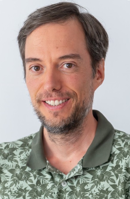
Luis A. Camuñas Mesa
Institute of Microelectronics of Seville (IMSE-CNM, CSIC)
Tuesday March 10, 18:00 to 19:00
“Neuromorphic Systems: Toward Sustainable AI”
Developing and deploying sophisticated AI models currently faces a critical energy bottleneck. Neuromorphic systems, modeled after the efficacy and robustness of natural biological intelligence, offer an energy-efficient alternative through massively parallel processing. Central to this paradigm is the emergence of nanoscale memristors, which, when coupled with conventional CMOS technology, allow for ultra-dense in-memory computing architectures. These hybrid CMOS-memristor systems utilize dense memristive crossbars to provide the synaptic connectivity necessary for neural layers. Consequently, these platforms serve as an ideal substrate for power-efficient online learning mechanisms, such as STDP, paving the way for the next generation of sustainable AI.
Biography:
Luis A. Camuñas Mesa is an Electronic Engineer from the University of Seville, Spain (2003), and holds a PhD in event-based vision systems from the same university (2010). In 2006, he was a Visiting Student with the Institute of Neuroinformatics, Zürich (Switzerland). From 2010 to 2013, he was an Associate Post-Doctoral Researcher with the Centre for Systems Neuroscience, University of Leicester (UK), where he was involved in olfactory sensing and processing, spike detection and sorting, and simulation of extracellular recordings. In 2013, he received the ‘Juan de la Cierva’ Post-Doctoral Fellowship at the Institute of Microelectronics of Seville (IMSE-CNM). In 2019, he became a Research Associate at the University of Seville. Since 2023, he holds a position as Tenured Scientist at CSIC (Spanish National Research Council). His current research interests include bioinspired circuits and systems, real-time event-based vision sensing and processing chips, neuromorphic stereo vision, and nanoscale memristor-based AER circuits for STDP learning. He has been an Associate Editor of the IEEE Transactions of Circuits and Systems – II: Express Briefs.

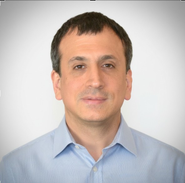
John H Lau
Unimicron Technology Corporation
Wednesday March 11, 18:00 to 19:00
“Co-Packaged Optics – 3D Heterogeneous Integration of Photonic IC and Electronic IC”
Co-packaged optics (CPO) are heterogeneous integration packaging methods to integrate the optical engine (OE) which consists of photonic ICs (PIC) and the electrical engine (EE) which consists of the electronic ICs (EIC) as well as the switch ASIC (application specific IC). The advantages of CPO are: (a) to reduce the length of the electrical interface between the OE/EE (or PIC/EIC) and the ASIC, (b) to reduce the energy required to drive the signal, and (c) to cut the latency which leads to better electrical performance. In the next few years, we will see more implementations of a higher level of heterogeneous integration of PIC and EIC, whether it is for performance, form factor, power consumption or cost. In this talk, 3D heterogeneous integration of ASIC switch, PIC, and EIC w/o bridges on organic, silicon, and glass substrate/interposer will be discussed. Some recommendations will be provided.
Biography:
John Lau with more than 40 years of R&D and manufacturing experience in semiconductor packaging, has published more than 530 peer-reviewed papers (385 as the principal investigator), 52 issued and pending US patents (31 as the principal inventor), and 25 textbooks. He has been actively participating in industry/academy/society meetings/conferences to contribute, learn, and share.

Mijal Mass
INTI y Julián Areso - FlexiiC
Thursday March 12, 18:30 to 19:30
“Introduction to printed electronics applications and organic integrated circuits”
Printed electronics is a technology that uses the same traditional graphic printing processes (inkjet, screen printing, flexography, etc.) to print electronic devices such as sensors, antennas, heaters, and other electronic circuits, commonly on flexible substrates. Likewise, organic electronics has proven to be a suitable technology for manufacturing devices on plastic and flexible substrates thanks to the possibility of producing low-cost, high-volume, high-performance components for electronic devices.
The combination of both technologies offers attractive solutions in which, among other elements, in situ monitoring of consumer goods, health monitoring patches, healthcare products such as smart bandages, and disposable sensors for food, pharmaceuticals, agriculture, and the environment could be integrated.
Biography:
Graduated in Electronic Engineering from the UTN-FRBA. Currently completing her PhD at ECyT at UNSAM, in the “Development of disposable biosensors with functional printing technology and hybridization of associated electronics”.
Since 2013 she has teaching Electronic Technology, of the Electronic Engineering course at UTN-FRBA.
Since 2009 she has been working at INTI in the area of Micro and Nanosystems and since 2013 she has participated in the creation of the Printed Electronics Laboratory. She has received training at national and international universities and institutes related to this subject, such as Eurecat-CETEMMSA, CNM-IMB in Spain and TU Chemnitz in Germany. From 2019, she has been responsible for the Microelectronic Prototyping and Printed Electronics Department, made up of a work team that carries out R&D activities in the area of Functional Printing, combining electronics, additive film deposition techniques, polymeric materials and 3D printing, for microelectronic devices and systems (sensors, biosensors, portable devices for medical and/or veterinary diagnosis, wearable systems and other electronic components) with the mission of fostering and promoting innovative technological solutions to reach the minimum viable product (MVP).
Félix Palumbo
CONICET-UTN-FRBA
Friday March 13, 17:00 to 18:00
“Dielectric Breakdown: From Fundamentals to Correlated Defect Generation in HfO2”
Thin dielectric films are essential components in modern microelectronics, and their reliability has become a critical challenge as market demands for device performance intensify. Understanding not only the physical phenomena behind dielectric breakdown but also its statistics is crucial for guaranteeing the reliability of current and future electronic devices.
This presentation will first review the fundamentals of the dielectric breakdown phenomenon in traditional and novel layered dielectrics. We will then delve into a specific investigation of breakdown statistics in HfO2, focusing on the dependence of the Weibull slope (β) on the initial defect density. This was analyzed using Time-Dependent Dielectric Breakdown (TDDB) tests on HfO2 MOS capacitors where defects were artificially induced via carefully tuned micro-beam irradiation.
Our results show a consistent experimental trend: the Weibull slope (β) decreases as the initial defect density increases. We demonstrate that conventional models based on spatially random defect distribution and generation fail to explain this trend. The experimental results were only reproducible with physics-based breakdown simulations that consider correlated defect generation and localized damage paths created by the impinging ions. This finding confirms that defect generation in HfO2 is not purely random, thereby altering the conventional understanding of TDDB and its significant implications for reliability modeling in advanced electronic devices.
Biography:
He is a Principal Device Engineer at Allegro MicroSystems with extensive academic and industrial experience in semiconductor device physics, reliability, and transport phenomena at material interfaces. He received his PhD (2005) and MSc (2000) in Physics from the University of Buenos Aires.
He has authored over 100 scientific papers (h-index: 24) with more than 2,295 citations and holds six U.S. patents. His work received the 2019 IEEE IRPS Best Paper Award, and he serves as an Editor for IEEE Transactions on Device and Materials Reliability and as an IEEE-EDS Distinguished Lecturer.
He is also a Full Professor at the National Technological University (UTN) in Buenos Aires, where he has led more than 25 funded research projects and supervised numerous PhD students. At Allegro, he focuses on bridging device physics and high-volume manufacturing, leading DOE definition, advanced electrical characterization, failure analysis, and BEOL design rule development to enhance yield and long-term reliability.
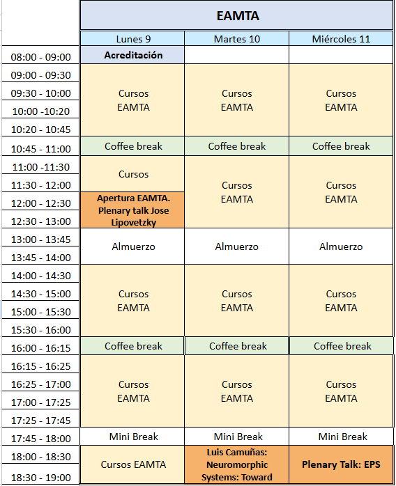
Schedule